Diffusion plate for line lightIKBB-LSR series
| Model | IKBB-LSR300-90 | IKBB-LSR300-80 | IKBB-LSR300-60 |
|---|---|---|---|
| Product Number | 617-032 | 617-033 | 617-034 |
| Transmittance | 90% | 80% | 60% |
| Light Used | |||
| Operating Temperature | 0~+40℃ | ||
| Operating Humidity | 35~70% (non condensing) | ||
| Weight | TBD | ||
| Conformity Standard | |||
| RoHS Directive |  |
||
| China RoHS |  |
||
IKBB-LSR200
Diffusion plate for line lightIKBB-LSR series
| Model | IKBB-LSR200-90 | IKBB-LSR200-80 | IKBB-LSR200-60 |
|---|---|---|---|
| Product Number | 617-022 | 617-023 | 617-024 |
| Transmittance | 90% | 80% | 60% |
| Light Used | |||
| Operating Temperature | 0~+40℃ | ||
| Operating Humidity | 35~70% (non condensing) | ||
| Weight | TBD | ||
| Conformity Standard | |||
| RoHS Directive | |
||
| China RoHS | |
||
IKBB-LSR100
Diffusion plate for line lightIKBB-LSR series
| Model | IKBB-LSR100-90 | IKBB-LSR100-80 | IKBB-LSR100-60 |
|---|---|---|---|
| Product Number | 617-012 | 617-013 | 617-014 |
| Transmittance | 90% | 80% | 60% |
| Light Used | |||
| Operating Temperature | 0~+40℃ | ||
| Operating Humidity | 35~70% (non condensing) | ||
| Weight | TBD | ||
| Conformity Standard | |||
| RoHS Directive | |
||
| China RoHS | |
||
IKBB-LSR series
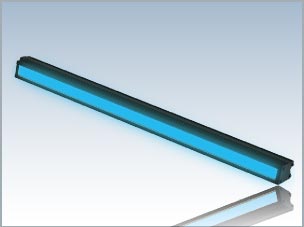
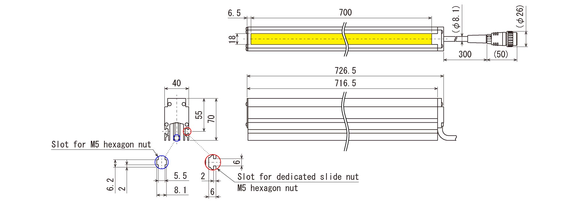
Diffusion plate for line illuminationIKBB-LSR series
IDBC-LSR1000_-S-IL
IDBC-LSR1000_-S-IL1.2 million lx Brimax line Illumination – IDBC-LSR series

| Model | IDBC-LSR1000R-S-IL | IDBC-LSR1000W-S-IL | IDBC-LSR1000B-S-IL | IDBC-LSR1000IR-860-S-IL |
|---|---|---|---|---|
| Product Number | 812-610 | 810-610 | 811-610 | 813-610 |
| Color |  |
 |
 |
 |
| Color temperature/Peak Wavelength | 634nm | 5700K typ. | 465nm | 860nm |
| Input Voltage | DC24V | |||
| Power Consumption | 150W | 200W | 200W | 160W |
| Cable Length | 300mm | |||
| Input Connector | Metal connector | |||
| Operating Temperature | 0~+40℃ | |||
| Operating Humidity | 35~85% (non condensing) | |||
| Weight | TBD | |||
| Conformity Standard |  IEC62471 |
|||
| RoHS Directive | |
|||
| China RoHS |  |
|||
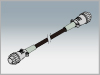
| Cables | ||||
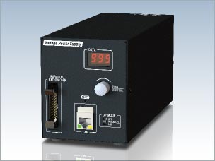
| Controllers | ||||
* Mass includes error.
IDBC-LSR900_-S-IL
IDBC-LSR900_-S-IL1.2 million lx Brimax line Illumination – IDBC-LSR series

| Model | IDBC-LSR900R-S-IL | IDBC-LSR900W-S-IL | IDBC-LSR900B-S-IL | IDBC-LSR900IR-860-S-IL |
|---|---|---|---|---|
| Product Number | 812-609 | 810-609 | 811-609 | 813-609 |
| Color | |
|
|
|
| Color temperature/Peak Wavelength | 634nm | 5700K typ. | 465nm | 860nm |
| Input Voltage | DC24V | |||
| Power Consumption | 135W | 180W | 180W | 144W |
| Cable Length | 300mm | |||
| Input Connector | Metal connector | |||
| Operating Temperature | 0~+40℃ | |||
| Operating Humidity | 35~85% (non condensing) | |||
| Weight | TBD | |||
| Conformity Standard | IEC62471 |
|||
| RoHS Directive | |
|||
| China RoHS | |
|||
| Cables | ||||
| Controllers | ||||
* Mass includes error.
IDBC-LSR800_-S-IL
IDBC-LSR800_-S-IL1.2 million lx Brimax line Illumination – IDBC-LSR series

| Model | IDBC-LSR800R-S-IL | IDBC-LSR800W-S-IL | IDBC-LSR800B-S-IL | IDBC-LSR800IR-860-S-IL |
|---|---|---|---|---|
| Product Number | 812-608 | 810-608 | 811-608 | 813-608 |
| Color | |
|
|
|
| Color temperature/Peak Wavelength | 634nm | 5700K typ. | 465nm | 860nm |
| Input Voltage | DC24V | |||
| Power Consumption | 120W | 160W | 160W | 128W |
| Cable Length | 300mm | |||
| Input Connector | Metal connector | |||
| Operating Temperature | 0~+40℃ | |||
| Operating Humidity | 35~85% (non condensing) | |||
| Weight | TBD | |||
| Conformity Standard | IEC62471 |
|||
| RoHS Directive | |
|||
| China RoHS | |
|||
| Cables | ||||
| Controllers | ||||
* Mass includes error.
IDBC-LSR700_-S-IL
IDBC-LSR700_-S-IL1.2 million lx Brimax line Illumination – IDBC-LSR series
| Model | IDBC-LSR700R-S-IL | IDBC-LSR700W-S-IL | IDBC-LSR700B-S-IL | IDBC-LSR700IR-860-S-IL |
|---|---|---|---|---|
| Product Number | 812-607 | 810-607 | 811-607 | 813-607 |
| Color | |
|
|
|
| Color temperature/Peak Wavelength | 634nm | 5700K typ. | 465nm | 860nm |
| Input Voltage | DC24V | |||
| Power Consumption | 105W | 140W | 140W | 112W |
| Cable Length | 300mm | |||
| Input Connector | Metal connector | |||
| Operating Temperature | 0~+40℃ | |||
| Operating Humidity | 35~85% (non condensing) | |||
| Weight | TBD | |||
| Conformity Standard | IEC62471 |
|||
| RoHS Directive | |
|||
| China RoHS | |
|||
| Cables | ||||
| Controllers | ||||
* Mass includes error.
IDBC-LSR600_-S-IL
IDBC-LSR600_-S-IL1.2 million lx Brimax line Illumination – IDBC-LSR series
| Model | IDBC-LSR600R-S-IL | IDBC-LSR600W-S-IL | IDBC-LSR600B-S-IL | IDBC-LSR600IR-860-S-IL |
|---|---|---|---|---|
| Product Number | 812-606 | 810-606 | 811-606 | 813-606 |
| Color | |
|
|
|
| Color temperature/Peak Wavelength | 634nm | 5700K typ. | 465nm | 860nm |
| Input Voltage | DC24V | |||
| Power Consumption | 90W | 120W | 120W | 96W |
| Cable Length | 300mm | |||
| Input Connector | Metal connector | |||
| Operating Temperature | 0~+40℃ | |||
| Operating Humidity | 35~85% (non condensing) | |||
| Weight | TBD | |||
| Conformity Standard | IEC62471 |
|||
| RoHS Directive | |
|||
| China RoHS | |
|||
| Cables | ||||
| Controllers | ||||
* Mass includes error.
IDBC-LSR500_-S-IL
IDBC-LSR500_-S-IL1.2 million lx Brimax line Illumination – IDBC-LSR series

| Model | IDBC-LSR500R-S-IL | IDBC-LSR500W-S-IL | IDBC-LSR500B-S-IL | IDBC-LSR500IR-860-S-IL |
|---|---|---|---|---|
| Product Number | 812-605 | 810-605 | 811-605 | 813-605 |
| Color | |
|
|
|
| Color temperature/Peak Wavelength | 634nm | 5700K typ. | 465nm | 860nm |
| Input Voltage | DC24V | |||
| Power Consumption | 75W | 100W | 100W | 80W |
| Cable Length | 300mm | |||
| Input Connector | Metal connector | |||
| Operating Temperature | 0~+40℃ | |||
| Operating Humidity | 35~85% (non condensing) | |||
| Weight | TBD | |||
| Conformity Standard | IEC62471 |
|||
| RoHS Directive | |
|||
| China RoHS | |
|||
| Cables | ||||
| Controllers | ||||
| Options |
Please select the option of the corresponding size. |
|||
* Mass includes error.
IDBC-LSR400_-S-IL
IDBC-LSR400_-S-IL1.2 million lx Brimax line Illumination – IDBC-LSR series

| Model | IDBC-LSR400R-S-IL | IDBC-LSR400W-S-IL | IDBC-LSR400B-S-IL | IDBC-LSR400IR-860-S-IL |
|---|---|---|---|---|
| Product Number | 812-604 | 810-604 | 811-604 | 813-604 |
| Color | |
|
|
|
| Color temperature/Peak Wavelength | 634nm | 5700K typ. | 465nm | 860nm |
| Input Voltage | DC24V | |||
| Power Consumption | 60W | 80W | 80W | 64W |
| Cable Length | 300mm | |||
| Input Connector | Metal connector | |||
| Operating Temperature | 0~+40℃ | |||
| Operating Humidity | 35~85% (non condensing) | |||
| Weight | TBD | |||
| Conformity Standard | IEC62471 |
|||
| RoHS Directive | |
|||
| China RoHS | |
|||
| Cables | ||||
| Controllers | ||||
| Options |
Please select the option of the corresponding size. |
|||
* Mass includes error.
IDBC-LSR300_-S-IL
IDBC-LSR300_-S-IL1.2 million lx Brimax line Illumination – IDBC-LSR series

| Model | IDBC-LSR300R-S-IL | IDBC-LSR300W-S-IL | IDBC-LSR300B-S-IL | IDBC-LSR300IR-860-S-IL |
|---|---|---|---|---|
| Product Number | 812-603 | 810-603 | 811-603 | 813-603 |
| Color | |
|
|
|
| Color temperature/Peak Wavelength | 634nm | 5700K typ. | 465nm | 860nm |
| Input Voltage | DC24V | |||
| Power Consumption | 45W | 60W | 60W | 48W |
| Cable Length | 300mm | |||
| Input Connector | Metal connector | |||
| Operating Temperature | 0~+40℃ | |||
| Operating Humidity | 35~85% (non condensing) | |||
| Weight | TBD | |||
| Conformity Standard | IEC62471 |
|||
| RoHS Directive | |
|||
| China RoHS | |
|||
| Cables | ||||
| Controllers | ||||
| Options |
Please select the option of the corresponding size. |
|||
* Mass includes error.
IDBC-LSR200_-S-IL
IDBC-LSR200_-S-IL1.2 million lx Brimax line Illumination – IDBC-LSR series

| Model | IDBC-LSR200R-S-IL | IDBC-LSR200W-S-IL | IDBC-LSR200B-S-IL | IDBC-LSR200IR-860-S-IL |
|---|---|---|---|---|
| Product Number | 812-602 | 810-602 | 811-602 | 813-602 |
| Color | |
|
|
|
| Color temperature/Peak Wavelength | 634nm | 5700K typ. | 465nm | 860nm |
| Input Voltage | DC24V | |||
| Power Consumption | 30W | 40W | 40W | 32W |
| Cable Length | 300mm | |||
| Input Connector | Metal connector | |||
| Operating Temperature | 0~+40℃ | |||
| Operating Humidity | 35~85% (non condensing) | |||
| Weight | TBD | |||
| Conformity Standard | IEC62471 |
|||
| RoHS Directive | |
|||
| China RoHS | |
|||
| Cables | ||||
| Controllers | ||||
| Options |
Please select the option of the corresponding size. |
|||
* Mass includes error.
IDBC-LSR100_-S-IL
IDBC-LSR100_-S-IL1.2 million lx Brimax line Illumination – IDBC-LSR series

| Model | IDBC-LSR100R-S-IL | IDBC-LSR100W-S-IL | IDBC-LSR100B-S-IL | IDBC-LSR100IR-860-S-IL |
|---|---|---|---|---|
| Product Number | 812-601 | 810-601 | 811-601 | 813-601 |
| Color | |
|
|
|
| Color temperature/Peak Wavelength | 634nm | 5700K typ. | 465nm | 860nm |
| Input Voltage | DC24V | |||
| Power Consumption | 15W | 20W | 20W | 16W |
| Cable Length | 300mm | |||
| Input Connector | Metal connector | |||
| Operating Temperature | 0~+40℃ | |||
| Operating Humidity | 35~85% (non condensing) | |||
| Weight | TBD | |||
| Conformity Standard | IEC62471 |
|||
| RoHS Directive | |
|||
| China RoHS | |
|||
| Cables | ||||
| Controllers | ||||
| Options |
Please select the option of the corresponding size. |
|||
* Mass includes error.
IDBC-LSR1000_-IL
IDBC-LSR1000_-IL1.2 million lx Brimax line Illumination – IDBC-LSR series
| Model | IDBC-LSR1000R-IL | IDBC-LSR1000W-IL | IDBC-LSR1000IR-860-IL |
|---|---|---|---|
| Product Number | 812-110 | 810-110 | 813-110 |
| Color | |
|
|
| Color temperature/Peak Wavelength | 634nm | 5700K typ. | 860nm |
| Input Voltage | DC24V | ||
| Power Consumption | 150W | 200W | 160W |
| Cable Length | 300mm | ||
| Input Connector | Metal connector | ||
| Operating Temperature | 0~+40℃ | ||
| Operating Humidity | 35~85% (non condensing) | ||
| Weight | TBD | ||
| Conformity Standard | IEC62471 |
||
| RoHS Directive | |
||
| China RoHS | |
||
| Cables | |||
| Controllers | |||
* Mass includes error.
IDBC-LSR900_-IL
IDBC-LSR900_-IL1.2 million lx Brimax line Illumination – IDBC-LSR series
| Model | IDBC-LSR900R-IL | IDBC-LSR900W-IL | IDBC-LSR900IR-860-IL |
|---|---|---|---|
| Product Number | 812-109 | 810-109 | 813-109 |
| Color | |
|
|
| Color temperature/Peak Wavelength | 634nm | 5700K typ. | 860nm |
| Input Voltage | DC24V | ||
| Power Consumption | 135W | 180W | 144W |
| Cable Length | 300mm | ||
| Input Connector | Metal connector | ||
| Operating Temperature | 0~+40℃ | ||
| Operating Humidity | 35~85% (non condensing) | ||
| Weight | TBD | ||
| Conformity Standard | IEC62471 |
||
| RoHS Directive | |
||
| China RoHS | |
||
| Cables | |||
| Controllers | |||
* Mass includes error.
IDBC-LSR800_-IL
IDBC-LSR800_-IL1.2 million lx Brimax line Illumination – IDBC-LSR series
| Model | IDBC-LSR800R-IL | IDBC-LSR800W-IL | IDBC-LSR800IR-860-IL |
|---|---|---|---|
| Product Number | 812-108 | 810-108 | 813-108 |
| Color | |
|
|
| Color temperature/Peak Wavelength | 634nm | 5700K typ. | 860nm |
| Input Voltage | DC24V | ||
| Power Consumption | 120W | 160W | 128W |
| Cable Length | 300mm | ||
| Input Connector | Metal connector | ||
| Operating Temperature | 0~+40℃ | ||
| Operating Humidity | 35~85% (non condensing) | ||
| Weight | TBD | ||
| Conformity Standard | IEC62471 |
||
| RoHS Directive | |
||
| China RoHS | |
||
| Cables | |||
| Controllers | |||
* Mass includes error.
IDBC-LSR700_-IL
IDBC-LSR700_-IL1.2 million lx Brimax line Illumination – IDBC-LSR series
| Model | IDBC-LSR700R-IL | IDBC-LSR700W-IL | IDBC-LSR700IR-860-IL |
|---|---|---|---|
| Product Number | 812-107 | 810-107 | 813-107 |
| Color | |
|
|
| Color temperature/Peak Wavelength | 634nm | 5700K typ. | 860nm |
| Input Voltage | DC24V | ||
| Power Consumption | 105W | 140W | 112W |
| Cable Length | 300mm | ||
| Input Connector | Metal connector | ||
| Operating Temperature | 0~+40℃ | ||
| Operating Humidity | 35~85% (non condensing) | ||
| Weight | TBD | ||
| Conformity Standard | IEC62471 |
||
| RoHS Directive | |
||
| China RoHS | |
||
| Cables | |||
| Controllers | |||
* Mass includes error.
IDBC-LSR600_-IL
IDBC-LSR600_-IL1.2 million lx Brimax line Illumination – IDBC-LSR series
| Model | IDBC-LSR600R-IL | IDBC-LSR600W-IL | IDBC-LSR600IR-860-IL |
|---|---|---|---|
| Product Number | 812-106 | 810-106 | 813-106 |
| Color | |
|
|
| Color temperature/Peak Wavelength | 634nm | 5700K typ. | 860nm |
| Input Voltage | DC24V | ||
| Power Consumption | 90W | 120W | 96W |
| Cable Length | 300mm | ||
| Input Connector | Metal connector | ||
| Operating Temperature | 0~+40℃ | ||
| Operating Humidity | 35~85% (non condensing) | ||
| Weight | TBD | ||
| Conformity Standard | IEC62471 |
||
| RoHS Directive | |
||
| China RoHS | |
||
| Cables | |||
| Controllers | |||
* Mass includes error.
IDBC-LSR500_-IL
IDBC-LSR500_-IL1.2 million lx Brimax line Illumination – IDBC-LSR series
| Model | IDBC-LSR500R-IL | IDBC-LSR500W-IL | IDBC-LSR500IR-860-IL |
|---|---|---|---|
| Product Number | 812-105 | 810-105 | 813-105 |
| Color | |
|
|
| Color temperature/Peak Wavelength | 634nm | 5700K typ. | 860nm |
| Input Voltage | DC24V | ||
| Power Consumption | 75W | 100W | 80W |
| Cable Length | 300mm | ||
| Input Connector | Metal connector | ||
| Operating Temperature | 0~+40℃ | ||
| Operating Humidity | 35~85% (non condensing) | ||
| Weight | TBD | ||
| Conformity Standard | IEC62471 |
||
| RoHS Directive | |
||
| China RoHS | |
||
| Cables | |||
| Controllers | |||
| Options |
Please select the option of the corresponding size. |
||
* Mass includes error.
IDBC-LSR400_-IL
IDBC-LSR400_-IL1.2 million lx Brimax line Illumination – IDBC-LSR series
| Model | IDBC-LSR400R-IL | IDBC-LSR400W-IL | IDBC-LSR400IR-860-IL |
|---|---|---|---|
| Product Number | 812-104 | 810-104 | 813-104 |
| Color | |
|
|
| Color temperature/Peak Wavelength | 634nm | 5700K typ. | 860nm |
| Input Voltage | DC24V | ||
| Power Consumption | 60W | 80W | 64W |
| Cable Length | 300mm | ||
| Input Connector | Metal connector | ||
| Operating Temperature | 0~+40℃ | ||
| Operating Humidity | 35~85% (non condensing) | ||
| Weight | TBD | ||
| Conformity Standard | IEC62471 |
||
| RoHS Directive | |
||
| China RoHS | |
||
| Cables | |||
| Controllers | |||
| Options |
Please select the option of the corresponding size. |
||
* Mass includes error.
IDBC-LSR300_-IL
IDBC-LSR300_-IL1.2 million lx Brimax line Illumination – IDBC-LSR series
| Model | IDBC-LSR300R-IL | IDBC-LSR300W-IL | IDBC-LSR300IR-860-IL |
|---|---|---|---|
| Product Number | 812-103 | 810-103 | 813-103 |
| Color | |
|
|
| Color temperature/Peak Wavelength | 634nm | 5700K typ. | 860nm |
| Input Voltage | DC24V | ||
| Power Consumption | 45W | 60W | 48W |
| Cable Length | 300mm | ||
| Input Connector | Metal connector | ||
| Operating Temperature | 0~+40℃ | ||
| Operating Humidity | 35~85% (non condensing) | ||
| Weight | TBD | ||
| Conformity Standard | IEC62471 |
||
| RoHS Directive | |
||
| China RoHS | |
||
| Cables | |||
| Controllers | |||
| Options |
Please select the option of the corresponding size. |
||
* Mass includes error.
IDBC-LSR200_-IL
IDBC-LSR200_-IL1.2 million lx Brimax line Illumination – IDBC-LSR series
| Model | IDBC-LSR200R-IL | IDBC-LSR200W-IL | IDBC-LSR200IR-860-IL |
|---|---|---|---|
| Product Number | 812-102 | 810-102 | 813-102 |
| Color | |
|
|
| Color temperature/Peak Wavelength | 634nm | 5700K typ. | 860nm |
| Input Voltage | DC24V | ||
| Power Consumption | 30W | 40W | 32W |
| Cable Length | 300mm | ||
| Input Connector | Metal connector | ||
| Operating Temperature | 0~+40℃ | ||
| Operating Humidity | 35~85% (non condensing) | ||
| Weight | TBD | ||
| Conformity Standard | IEC62471 |
||
| RoHS Directive | |
||
| China RoHS | |
||
| Cables | |||
| Controllers | |||
| Options |
Please select the option of the corresponding size. |
||
* Mass includes error.
IDBC-LSR100_-IL
IDBC-LSR100_-IL1.2 million lx Brimax line Illumination – IDBC-LSR series
| Model | IDBC-LSR100R-IL | IDBC-LSR100W-IL | IDBC-LSR100IR-860-IL |
|---|---|---|---|
| Product Number | 812-101 | 810-101 | 813-101 |
| Color | |
|
|
| Color temperature/Peak Wavelength | 634nm | 5700K typ. | 860nm |
| Input Voltage | DC24V | ||
| Power Consumption | 15W | 20W | 16W |
| Cable Length | 300mm | ||
| Input Connector | Metal connector | ||
| Operating Temperature | 0~+40℃ | ||
| Operating Humidity | 35~85% (non condensing) | ||
| Weight | TBD | ||
| Conformity Standard | IEC62471 |
||
| RoHS Directive | |
||
| China RoHS | |
||
| Cables | |||
| Controllers | |||
| Options |
Please select the option of the corresponding size. |
||
* Mass includes error.
IDBC-LSR1500_-S
IDBC-LSR1500_-S1.2 million lx Brimax line Illumination – IDBC-LSR series
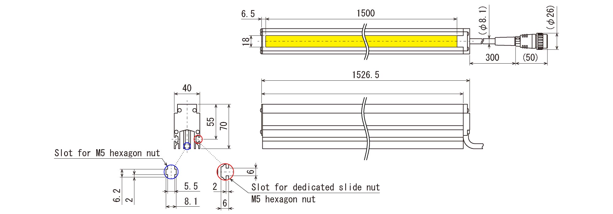
| Model | IDBC-LSR1500R-S | IDBC-LSR1500W-S | IDBC-LSR1500B-S | IDBC-LSR1500IR-860-S |
|---|---|---|---|---|
| Product Number | 812-515 | 810-515 | 811-515 | 813-515 |
| Color | |
|
|
|
| Color temperature/Peak Wavelength | 634nm | 5700K typ. | 465nm | 860nm |
| Input Voltage | DC24V | |||
| Power Consumption | 225W | 300W | 300W | 240W |
| Cable Length | 300mm | |||
| Input Connector | Metal connector | |||
| Polarity | – | |||
| Operating Temperature | 0~+40℃ | |||
| Operating Humidity | 35~85% (non condensing) | |||
| Weight | TBD | |||
| Conformity Standard | IEC62471 |
|||
| RoHS Directive | |
|||
| China RoHS | |
|||
| Cables | ||||
| Controllers | ||||
* In addition to the above sizes, luminous surface lengths from 100 to 1500 (in increments of 100 mm) can also be manufactured.
* Mass includes error.
IDBC-LSR1400_-S
IDBC-LSR1400_-S1.2 million lx Brimax line Illumination – IDBC-LSR series

| Model | IDBC-LSR1400R-S | IDBC-LSR1400W-S | IDBC-LSR1400B-S | IDBC-LSR1400IR-860-S |
|---|---|---|---|---|
| Product Number | 812-514 | 810-514 | 811-514 | 813-514 |
| Color | |
|
|
|
| Color temperature/Peak Wavelength | 634nm | 5700K typ. | 465nm | 860nm |
| Input Voltage | DC24V | |||
| Power Consumption | 210W | 280W | 280W | 224W |
| Cable Length | 300mm | |||
| Input Connector | Metal connector | |||
| Polarity | – | |||
| Operating Temperature | 0~+40℃ | |||
| Operating Humidity | 35~85% (non condensing) | |||
| Weight | TBD | |||
| Conformity Standard | IEC62471 |
|||
| RoHS Directive | |
|||
| China RoHS | |
|||
| Cables | ||||
| Controllers | ||||
* In addition to the above sizes, luminous surface lengths from 100 to 1500 (in increments of 100 mm) can also be manufactured.
* Mass includes error.
IDBC-LSR1300_-S
IDBC-LSR1300_-S1.2 million lx Brimax line Illumination – IDBC-LSR series

| Model | IDBC-LSR1300R-S | IDBC-LSR1300W-S | IDBC-LSR1300B-S | IDBC-LSR1300IR-860-S |
|---|---|---|---|---|
| Product Number | 812-513 | 810-513 | 811-513 | 813-513 |
| Color | |
|
|
|
| Color temperature/Peak Wavelength | 634nm | 5700K typ. | 465nm | 860nm |
| Input Voltage | DC24V | |||
| Power Consumption | 195W | 260W | 260W | 208W |
| Cable Length | 300mm | |||
| Input Connector | Metal connector | |||
| Polarity | – | |||
| Operating Temperature | 0~+40℃ | |||
| Operating Humidity | 35~85% (non condensing) | |||
| Weight | TBD | |||
| Conformity Standard | IEC62471 |
|||
| RoHS Directive | |
|||
| China RoHS | |
|||
| Cables | ||||
| Controllers | ||||
* In addition to the above sizes, luminous surface lengths from 100 to 1500 (in increments of 100 mm) can also be manufactured.
* Mass includes error.
IDBC-LSR1200_-S
IDBC-LSR1200_-S1.2 million lx Brimax line Illumination – IDBC-LSR series

| Model | IDBC-LSR1200R-S | IDBC-LSR1200W-S | IDBC-LSR1200B-S | IDBC-LSR1200IR-860-S |
|---|---|---|---|---|
| Product Number | 812-512 | 810-512 | 811-512 | 813-512 |
| Color | |
|
|
|
| Color temperature/Peak Wavelength | 634nm | 5700K typ. | 465nm | 860nm |
| Input Voltage | DC24V | |||
| Power Consumption | 180W | 240W | 240W | 192W |
| Cable Length | 300mm | |||
| Input Connector | Metal connector | |||
| Polarity | – | |||
| Operating Temperature | 0~+40℃ | |||
| Operating Humidity | 35~85% (non condensing) | |||
| Weight | TBD | |||
| Conformity Standard | IEC62471 |
|||
| RoHS Directive | |
|||
| China RoHS | |
|||
| Cables | ||||
| Controllers | ||||
* In addition to the above sizes, luminous surface lengths from 100 to 1500 (in increments of 100 mm) can also be manufactured.
* Mass includes error.
IDBC-LSR1100_-S
IDBC-LSR1100_-S1.2 million lx Brimax line Illumination – IDBC-LSR series

| Model | IDBC-LSR1100R-S | IDBC-LSR1100W-S | IDBC-LSR1100B-S | IDBC-LSR1100IR-860-S |
|---|---|---|---|---|
| Product Number | 812-511 | 810-511 | 811-511 | 813-511 |
| Color | |
|
|
|
| Color temperature/Peak Wavelength | 634nm | 5700K typ. | 465nm | 860nm |
| Input Voltage | DC24V | |||
| Power Consumption | 165W | 220W | 220W | 176W |
| Cable Length | 300mm | |||
| Input Connector | Metal connector | |||
| Polarity | – | |||
| Operating Temperature | 0~+40℃ | |||
| Operating Humidity | 35~85% (non condensing) | |||
| Weight | TBD | |||
| Conformity Standard | IEC62471 |
|||
| RoHS Directive | |
|||
| China RoHS | |
|||
| Cables | ||||
| Controllers | ||||
* In addition to the above sizes, luminous surface lengths from 100 to 1500 (in increments of 100 mm) can also be manufactured.
* Mass includes error.
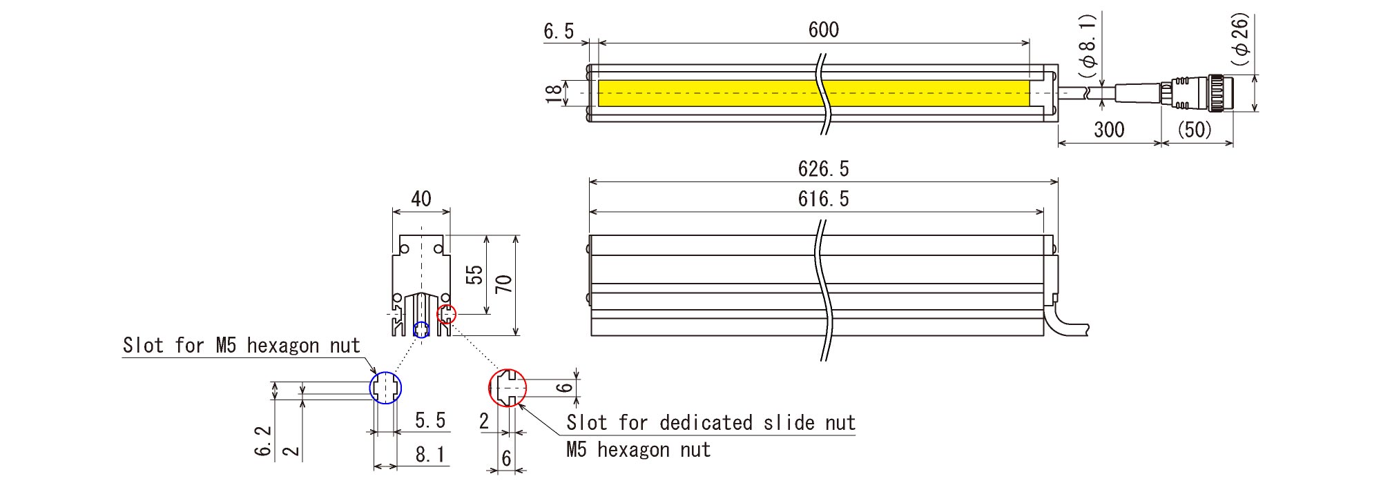
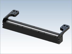
IDBC-LSR1000_-S
IDBC-LSR1000_-S1.2 million lx Brimax line Illumination – IDBC-LSR series
| Model | IDBC-LSR1000R-S | IDBC-LSR1000W-S | IDBC-LSR1000B-S | IDBC-LSR1000IR-860-S |
|---|---|---|---|---|
| Product Number | 812-510 | 810-510 | 811-510 | 813-510 |
| Color | |
|
|
|
| Color temperature/Peak Wavelength | 634nm | 5700K typ. | 465nm | 860nm |
| Input Voltage | DC24V | |||
| Power Consumption | 150W | 200W | 200W | 160W |
| Cable Length | 300mm | |||
| Input Connector | Metal connector | |||
| Polarity | – | |||
| Operating Temperature | 0~+40℃ | |||
| Operating Humidity | 35~85% (non condensing) | |||
| Weight | TBD | |||
| Conformity Standard | IEC62471 |
|||
| RoHS Directive | |
|||
| China RoHS | |
|||
| Cables | ||||
| Controllers | ||||
* In addition to the above sizes, luminous surface lengths from 100 to 1500 (in increments of 100 mm) can also be manufactured.
* Mass includes error.
IDBC-LSR900_-S
IDBC-LSR900_-S1.2 million lx Brimax line Illumination – IDBC-LSR series
| Model | IDBC-LSR900R-S | IDBC-LSR900W-S | IDBC-LSR900B-S | IDBC-LSR900IR-860-S |
|---|---|---|---|---|
| Product Number | 812-509 | 810-509 | 811-509 | 813-509 |
| Color | |
|
|
|
| Color temperature/Peak Wavelength | 634nm | 5700K typ. | 465nm | 860nm |
| Input Voltage | DC24V | |||
| Power Consumption | 135W | 180W | 180W | 144W |
| Cable Length | 300mm | |||
| Input Connector | Metal connector | |||
| Polarity | – | |||
| Operating Temperature | 0~+40℃ | |||
| Operating Humidity | 35~85% (non condensing) | |||
| Weight | TBD | |||
| Conformity Standard | IEC62471 |
|||
| RoHS Directive | |
|||
| China RoHS | |
|||
| Cables | ||||
| Controllers | ||||
* In addition to the above sizes, luminous surface lengths from 100 to 1500 (in increments of 100 mm) can also be manufactured.
* Mass includes error.
IDBC-LSR800_-S
IDBC-LSR800_-S1.2 million lx Brimax line Illumination – IDBC-LSR series
| Model | IDBC-LSR800R-S | IDBC-LSR800W-S | IDBC-LSR800B-S | IDBC-LSR800IR-860-S |
|---|---|---|---|---|
| Product Number | 812-508 | 810-508 | 811-508 | 813-508 |
| Color | |
|
|
|
| Color temperature/Peak Wavelength | 634nm | 5700K typ. | 465nm | 860nm |
| Input Voltage | DC24V | |||
| Power Consumption | 120W | 160W | 160W | 128W |
| Cable Length | 300mm | |||
| Input Connector | Metal connector | |||
| Polarity | – | |||
| Operating Temperature | 0~+40℃ | |||
| Operating Humidity | 35~85% (non condensing) | |||
| Weight | TBD | |||
| Conformity Standard | IEC62471 |
|||
| RoHS Directive | |
|||
| China RoHS | |
|||
| Cables | ||||
| Controllers | ||||
* In addition to the above sizes, luminous surface lengths from 100 to 1500 (in increments of 100 mm) can also be manufactured.
* Mass includes error.
IDBC-LSR700_-S
IDBC-LSR700_-S1.2 million lx Brimax line Illumination – IDBC-LSR series
| Model | IDBC-LSR700R-S | IDBC-LSR700W-S | IDBC-LSR700B-S | IDBC-LSR700IR-860-S |
|---|---|---|---|---|
| Product Number | 812-507 | 810-507 | 811-507 | 813-507 |
| Color | |
|
|
|
| Color temperature/Peak Wavelength | 634nm | 5700K typ. | 465nm | 860nm |
| Input Voltage | DC24V | |||
| Power Consumption | 105W | 140W | 140W | 112W |
| Cable Length | 300mm | |||
| Input Connector | Metal connector | |||
| Polarity | – | |||
| Operating Temperature | 0~+40℃ | |||
| Operating Humidity | 35~85% (non condensing) | |||
| Weight | TBD | |||
| Conformity Standard | IEC62471 |
|||
| RoHS Directive | |
|||
| China RoHS | |
|||
| Cables | ||||
| Controllers | ||||
* In addition to the above sizes, luminous surface lengths from 100 to 1500 (in increments of 100 mm) can also be manufactured.
* Mass includes error.
IDBC-LSR600_-S
IDBC-LSR600_-S1.2 million lx Brimax line Illumination – IDBC-LSR series
| Model | IDBC-LSR600R-S | IDBC-LSR600W-S | IDBC-LSR600B-S | IDBC-LSR600IR-860-S |
|---|---|---|---|---|
| Product Number | 812-506 | 810-506 | 811-506 | 813-506 |
| Color | |
|
|
|
| Color temperature/Peak Wavelength | 634nm | 5700K typ. | 465nm | 860nm |
| Input Voltage | DC24V | |||
| Power Consumption | 90W | 120W | 120W | 96W |
| Cable Length | 300mm | |||
| Input Connector | Metal connector | |||
| Polarity | – | |||
| Operating Temperature | 0~+40℃ | |||
| Operating Humidity | 35~85% (non condensing) | |||
| Weight | 2060g | |||
| Conformity Standard | IEC62471 |
|||
| RoHS Directive | |
|||
| China RoHS | |
|||
| Cables | ||||
| Controllers | ||||
* In addition to the above sizes, luminous surface lengths from 100 to 1500 (in increments of 100 mm) can also be manufactured.
* Mass includes error.
IDBC-LSR500_-S
IDBC-LSR500_-S1.2 million lx Brimax line Illumination – IDBC-LSR series
| Model | IDBC-LSR500R-S | IDBC-LSR500W-S | IDBC-LSR500B-S | IDBC-LSR500IR-860-S |
|---|---|---|---|---|
| Product Number | 812-505 | 810-505 | 811-505 | 813-505 |
| Color | |
|
|
|
| Color temperature/Peak Wavelength | 634nm | 5700K typ. | 465nm | 860nm |
| Input Voltage | DC24V | |||
| Power Consumption | 75W | 100W | 100W | 80W |
| Cable Length | 300mm | |||
| Input Connector | Metal connector | |||
| Polarity | – | |||
| Operating Temperature | 0~+40℃ | |||
| Operating Humidity | 35~85% (non condensing) | |||
| Weight | TBD | |||
| Conformity Standard | IEC62471 |
|||
| RoHS Directive | |
|||
| China RoHS | |
|||
| Cables | ||||
| Controllers | ||||
| Options |
Please select the option of the corresponding size. |
|||
* In addition to the above sizes, luminous surface lengths from 100 to 1500 (in increments of 100 mm) can also be manufactured.
* Mass includes error.
IDBC-LSR400_-S
IDBC-LSR400_-S1.2 million lx Brimax line Illumination – IDBC-LSR series
| Model | IDBC-LSR400R-S | IDBC-LSR400W-S | IDBC-LSR400B-S | IDBC-LSR400IR-860-S |
|---|---|---|---|---|
| Product Number | 812-504 | 810-504 | 811-504 | 813-504 |
| Color | |
|
|
|
| Color temperature/Peak Wavelength | 634nm | 5700K typ. | 465nm | 860nm |
| Input Voltage | DC24V | |||
| Power Consumption | 60W | 80W | 80W | 64W |
| Cable Length | 300mm | |||
| Input Connector | Metal connector | |||
| Polarity | – | |||
| Operating Temperature | 0~+40℃ | |||
| Operating Humidity | 35~85% (non condensing) | |||
| Weight | 1435g | |||
| Conformity Standard | IEC62471 |
|||
| RoHS Directive | |
|||
| China RoHS | |
|||
| Cables | ||||
| Controllers | ||||
| Options |
Please select the option of the corresponding size. |
|||
* In addition to the above sizes, luminous surface lengths from 100 to 1500 (in increments of 100 mm) can also be manufactured.
* Mass includes error.
IDBC-LSR300_-S
IDBC-LSR300_-S1.2 million lx Brimax line Illumination – IDBC-LSR series
| Model | IDBC-LSR300R-S | IDBC-LSR300W-S | IDBC-LSR300B-S | IDBC-LSR300IR-860-S |
|---|---|---|---|---|
| Product Number | 812-503 | 810-503 | 811-503 | 813-503 |
| Color | |
|
|
|
| Color temperature/Peak Wavelength | 634nm | 5700K typ. | 465nm | 860nm |
| Input Voltage | DC24V | |||
| Power Consumption | 45W | 60W | 60W | 48W |
| Cable Length | 300mm | |||
| Input Connector | Metal connector | |||
| Polarity | – | |||
| Operating Temperature | 0~+40℃ | |||
| Operating Humidity | 35~85% (non condensing) | |||
| Weight | 1120g | |||
| Conformity Standard | IEC62471 |
|||
| RoHS Directive | |
|||
| China RoHS | |
|||
| Cables | ||||
| Controllers | ||||
| Options |
Please select the option of the corresponding size. |
|||
* In addition to the above sizes, luminous surface lengths from 100 to 1500 (in increments of 100 mm) can also be manufactured.
* Mass includes error.
IDBC-LSR200_-S
IDBC-LSR200_-S1.2 million lx Brimax line Illumination – IDBC-LSR series
| Model | IDBC-LSR200R-S | IDBC-LSR200W-S | IDBC-LSR200B-S | IDBC-LSR200IR-860-S |
|---|---|---|---|---|
| Product Number | 812-502 | 810-502 | 811-502 | 813-502 |
| Color | |
|
|
|
| Color temperature/Peak Wavelength | 634nm | 5700K typ. | 465nm | 860nm |
| Input Voltage | DC24V | |||
| Power Consumption | 30W | 40W | 40W | 32W |
| Cable Length | 300mm | |||
| Input Connector | Metal connector | |||
| Polarity | – | |||
| Operating Temperature | 0~+40℃ | |||
| Operating Humidity | 35~85% (non condensing) | |||
| Weight | 805g | |||
| Conformity Standard | IEC62471 |
|||
| RoHS Directive | |
|||
| China RoHS | |
|||
| Cables | ||||
| Controllers | ||||
| Options |
Please select the option of the corresponding size. |
|||
* In addition to the above sizes, luminous surface lengths from 100 to 1500 (in increments of 100 mm) can also be manufactured.
* Mass includes error.
IDBC-LSR100_-S
IDBC-LSR100_-S1.2 million lx Brimax line Illumination – IDBC-LSR series
| Model | IDBC-LSR100R-S | IDBC-LSR100W-S | IDBC-LSR100B-S | IDBC-LSR100IR-860-S |
|---|---|---|---|---|
| Product Number | 812-501 | 810-501 | 811-501 | 813-501 |
| Color | |
|
|
|
| Color temperature/Peak Wavelength | 634nm | 5700K typ. | 465nm | 860nm |
| Input Voltage | DC24V | |||
| Power Consumption | 15W | 20W | 20W | 16W |
| Cable Length | 300mm | |||
| Input Connector | Metal connector | |||
| Polarity | – | |||
| Operating Temperature | 0~+40℃ | |||
| Operating Humidity | 35~85% (non condensing) | |||
| Weight | 490g | |||
| Conformity Standard | IEC62471 |
|||
| RoHS Directive | |
|||
| China RoHS | |
|||
| Cables | ||||
| Controllers | ||||
| Options |
Please select the option of the corresponding size. |
|||
* In addition to the above sizes, luminous surface lengths from 100 to 1500 (in increments of 100 mm) can also be manufactured.
* Mass includes error.
IDBC-LSR1500
IDBC-LSR15001.2 million lx Brimax line Illumination – IDBC-LSR series
| Model | IDBC-LSR1500R | IDBC-LSR1500W | IDBC-LSR1500IR-860 |
|---|---|---|---|
| Product Number | 812-015 | 810-015 | 813-015 |
| Color | |
|
|
| Color temperature/Peak Wavelength | 634nm | 5700K typ. | 860nm |
| Input Voltage | DC24V | ||
| Power Consumption | 225W | 300W | 240W |
| Cable Length | 300mm | ||
| Input Connector | Metal connector | ||
| Polarity | – | ||
| Operating Temperature | 0~+40℃ | ||
| Operating Humidity | 35~85% (non condensing) | ||
| Weight | TBD | ||
| Conformity Standard | IEC62471 |
||
| RoHS Directive | |
||
| China RoHS | |
||
| Cables | |||
| Controllers | |||
| Options |
Please select the option of the corresponding size. |
||
* In addition to the above sizes, luminous surface lengths from 100 to 1500 (in increments of 100 mm) can also be manufactured.
* Mass includes error.
![]()
© Leimac Ltd. All Rights Reserved.
